- 您现在的位置:买卖IC网 > Sheet目录996 > NCP1351LEDGEVB (ON Semiconductor)EVAL BOARD FOR NCP1351LEDG
�� �
�
�NCP1351�
�Let� us� round� it� to� 0.25� or� 1/N� =� 4�
�From� Equation� 17,� a� K� factor� of� 0.8� (40%� ripple)� ensures� a�
�good� operation� over� universal� mains.� It� leads� to� an�
�inductance� of:�
�I� peak�
�L� +�
�(100�
�65� k�
�43)2�
�0.8� 72�
�+� 493� m� H�
�(eq.� 23)�
�I� 1�
�D� I� L�
�D� IL� +�
�Vin_mind max�
�LFSW�
�+�
�100�
�493� u�
�0.43�
�65� k�
�(eq.� 24)�
�+� 1.34� A� peak-to-peak�
�I� valley�
�The� peak� current� can� be� evaluated� to� be:�
�Iin_avg� +�
�Pout�
�h� Vin_min�
�+�
�19�
�0.8�
�3�
�100�
�+� 712� mA�
�(eq.� 25)�
�I� avg�
�Ipeak� +�
�Iavg�
�d�
�)�
�D� IL�
�2�
�+�
�0.712�
�0.43�
�)�
�1.34�
�2�
�+� 2.33� A�
�(eq.� 26)�
�t�
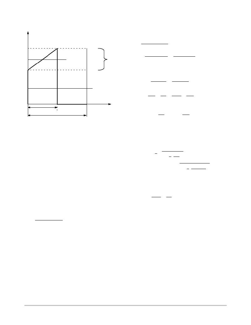
�On� Figure� 26,� I� 1� can� also� be� calculated:�
�DT� SW�
�T� SW�
�II� +� Ipeak� *�
�D� IL�
�2�
�+� 2.33� *�
�1.34�
�2�
�+� 1.65� A�
�(eq.� 27)�
�Figure� 26.� Primary� Inductance� Current� Evolution�
�The� valley� current� is� also� found� to� be:�
�in� CCM�
�Ivalley� +� Ipeak� *� D� IL� +� 2.33� *� 1.34� +� 1.0� A�
�(eq.� 28)�
�2.� Calculate� the� maximum� operating� duty-cycle� for�
�this� flyback� converter� operated� in� CCM:�
�4.� Based� on� the� above� numbers,� we� can� now� evaluate�
�the� RMS� current� circulating� in� the� MOSFET� and�
�the� sense� resistor:�
�d� max� +�
�Vout� N�
�Vout� N� )� Vin_min�
�+�
�19�
�19� 4�
�4� )� 100�
�+� 0.43�
�(eq.� 21)�
�Id_rms� +� II� d�
�1� )�
�1� D� IL� 2�
�3� 2I1�
�In� this� equation,� the� CCM� duty-cycle� does� not� exceed�
�50%.� The� design� should� thus� be� free� of� subharmonic�
�+� 1.65�
�0.65�
�1� )�
�1�
�3� 2�
�1.34�
�1.65�
�2�
�(eq.� 29)�
�oscillations� in� steady-state� conditions.� If� necessary,�
�negative� ramp� compensation� is� however� feasible� by� the�
�auxiliary� winding.�
�3.� To� obtain� the� primary� inductance,� we� can� use� the�
�+� 1.1� A�
�5.� The� current� peaks� to� 2.33� A.� Selecting� a� 1� V� drop�
�across� the� sense� resistor,� we� can� compute� its� value:�
�following� equation� which� expresses� the� inductance�
�in� relationship� to� a� coefficient� k.� This� coefficient�
�Rsense� +�
�1�
�Ipeak�
�+�
�1�
�2.5�
�+� 0.4� W�
�(eq.� 30)�
�L� +�
�actually� dictates� the� depth� of� the� CCM� operation.�
�If� it� goes� to� 2,� then� we� are� in� DCM.�
�(Vin_mind max)2�
�(eq.� 22)�
�FSWKPin�
�To� generate� 1� V,� the� offset� resistor� will� be� 3.7� k� W� ,� as� already�
�explained.� Using� Equation� 29,� the� power� dissipated� in� the�
�sense� element� reaches:�
�Psense� +� Rsense� Id_rms2� +� 0.4� 1.12� +� 484� mW�
�where� K� =� D� I� L� /I� I� and� defines� the� amount� of� ripple� we� want�
�in� CCM� (see� Figure� 26).�
�?� Small� K:� deep� CCM,� implying� a� large� primary�
�inductance,� a� low� bandwidth� and� a� large� leakage�
�inductance.�
�?� Large� K:� approaching� BCM� where� the� RMS� losses� are�
�the� worse,� but� smaller� inductance,� leading� to� a� better�
�leakage� inductance.�
�(eq.� 31)�
�6.� To� switch� at� 65� kHz,� the� C� t� capacitor� connected� to�
�pin� 2� will� be� selected� to� 180� pF.�
�7.� As� the� load� changes,� the� operating� frequency� will�
�automatically� adjust� to� satisfy� either� equation� 5�
�(high� power,� CCM)� or� equation� 6� in� lighter� load�
�conditions� (DCM).�
�Figure� 27� portrays� a� possible� application� schematic�
�implementing� what� we� discussed� in� the� above� lines.�
�http://onsemi.com�
�20�
�发布紧急采购,3分钟左右您将得到回复。
相关PDF资料
NCP3065BBGEVB
BOARD EVAL NCP3065 MR16 BOOST
NCP3066SCBCKGEVB
EVAL BOARD FOR NCP3066SCBCKG
NCP5005GEVB
EVAL BOARD FOR NCP5005G
NCP5006EVB
EVAL BOARD FOR NCP5006
NCP5030MTTXGEVB
EVAL BOARD FOR NCP5030MTTXG
NCP5602EVB
EVAL BOARD FOR NCP5602
NCP5603GEVB
EVAL BOARD FOR NCP5603G HI FREQ
NCP5604AAGEVB
EVAL BOARD FOR NCP5604AAG
相关代理商/技术参数
NCP1351PRINTGEVB
功能描述:电源管理IC开发工具 NCP1351 40 W PRINTER EVB
RoHS:否 制造商:Maxim Integrated 产品:Evaluation Kits 类型:Battery Management 工具用于评估:MAX17710GB 输入电压: 输出电压:1.8 V
NCP1377
制造商:ONSEMI 制造商全称:ON Semiconductor 功能描述:PWM Current-Mode Controller for Free-Running Quasi-Resonant Operation
NCP1377/D
制造商:未知厂家 制造商全称:未知厂家 功能描述:PWM Current -Mode Controller
NCP1377_06
制造商:ONSEMI 制造商全称:ON Semiconductor 功能描述:PWM Current−Mode Controller for Free−Running Quasi−Resonant Operation
NCP1377_11
制造商:ONSEMI 制造商全称:ON Semiconductor 功能描述:PWM Current-Mode Controller for Free-Running Quasi-Resonant Operation
NCP1377B
制造商:ONSEMI 制造商全称:ON Semiconductor 功能描述:PWM Current-Mode Controller for Free-Running Quasi-Resonant Operation
NCP1377BD1R2G
功能描述:电流型 PWM 控制器 ANA PWM CURRNT MODE CNTR RoHS:否 制造商:Texas Instruments 开关频率:27 KHz 上升时间: 下降时间: 工作电源电压:6 V to 15 V 工作电源电流:1.5 mA 输出端数量:1 最大工作温度:+ 105 C 安装风格:SMD/SMT 封装 / 箱体:TSSOP-14
NCP1377BDR2
功能描述:电流型 PWM 控制器 Quasi Resonant RoHS:否 制造商:Texas Instruments 开关频率:27 KHz 上升时间: 下降时间: 工作电源电压:6 V to 15 V 工作电源电流:1.5 mA 输出端数量:1 最大工作温度:+ 105 C 安装风格:SMD/SMT 封装 / 箱体:TSSOP-14